The idea: add hardware one instruction at a time
A processor's datapath is the hardware that moves and computes the data: memories, registers, the ALU, and the wires and muxes between them. Harris and Harris build the single-cycle MIPS datapath the way a designer would. They start with the parts that hold state, then take one instruction, lw, and add only what it needs. Then they take sw and R-type instructions and add what is still missing. This page animates those steps (Figures 7.2 to 7.9 of the book).
Press Next Step to add one figure's worth of hardware. In each step the wires added in that step are black, and the wire carrying the value right now pulses red. Hardware from earlier steps turns grey, as in the book. Blue lines are control signals. Purple numbers are the values on the wires. A register or memory word that is written at the clock edge turns green.
Start with the state elements
Four parts hold state: the PC (the address of the current instruction), the instruction memory, the register file (32 registers, two read ports, one write port) and the data memory. Reads are combinational: put an address on A and the data appears on RD. Writes happen only at the rising clock edge (the CLK triangle), and only when the write enable (WE3, WE) is 1. Everything added later is combinational logic between these four.
lw: six steps
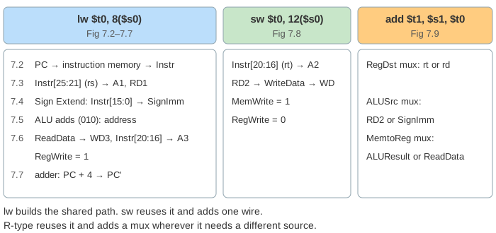
lw $t0, 8($s0) loads the word at address $s0 + 8 into $t0. Its machine code is 0x8E080008: op = 35, rs = 16 ($s0), rt = 8 ($t0), imm = 8. Demo: lw, piece by piece runs these steps.
| Figure | Hardware added | Value on the canvas |
|---|---|---|
| 7.2 | PC → A of the instruction memory, RD → Instr | Instr = 0x8E080008 |
| 7.3 | Instr[25:21] (rs) → A1, RD1 out | RD1 = $s0 = 0x100 |
| 7.4 | Sign Extend on Instr[15:0] | SignImm = 0x00000008 |
| 7.5 | ALU with ALUControl = 010 (add), ALUResult → A of the data memory | ALUResult = 0x108 |
| 7.6 | ReadData → WD3, Instr[20:16] (rt) → A3, RegWrite = 1 | $t0 ← 42 at the edge |
| 7.7 | an adder: PCPlus4 = PC + 4 → PC' | PC ← 0x04 at the edge |
Two details matter. The offset is sign-extended: bit 15 is copied into the upper 16 bits, so a negative offset like -4 (0xFFFC) becomes 0xFFFFFFFC, not 0x0000FFFC. And the PC adds 4, not 1, because MIPS memory is byte-addressed and each instruction is 4 bytes. All of this settles within one clock cycle; the register write and the PC update happen together at the next rising edge.
sw: one more wire
sw $t0, 12($s0) computes its address exactly like lw: $s0 + 12 = 0x10C. The only new thing is the data to store. sw reads a second register, rt, through the second read port: Instr[20:16] → A2, and RD2 → WD of the data memory. That wire is called WriteData. Two control signals make it a store: MemWrite = 1 lets memory write at the edge, and RegWrite = 0 keeps the register file unchanged (Demo: sw adds WriteData).
R-type: three muxes
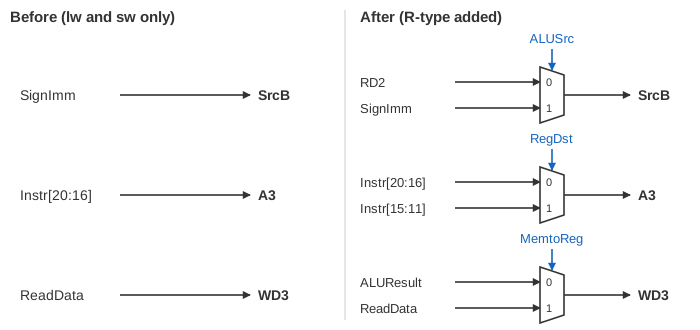
add $t1, $s1, $t0 (0x02284820) reads rs and rt, adds them, and writes rd. In three places it needs a different source than lw, so a 2:1 multiplexer is added at each, with a control line that picks the input (Demo: R-type adds three muxes):
| Mux | Input 0 | Input 1 | add uses | lw uses |
|---|---|---|---|---|
RegDst → WriteReg (A3) | Instr[20:16] (rt) | Instr[15:11] (rd) | 1 | 0 |
ALUSrc → SrcB | RD2 | SignImm | 0 | 1 |
MemtoReg → Result (WD3) | ALUResult | ReadData | 0 | 1 |
The ALU now does more than add. For R-type, ALUControl comes from the funct field (bits 5:0): 32 is add, so the ALU gets 010; sub would give 110, and 000, or 001, slt 111.
Where the control signals come from
After step 8 the datapath has six control lines: three mux selects and two write enables, plus the ALU's operation. Each instruction is just one setting of them. That table is the main decoder of the Control Unit, which the next section of the book builds from the opcode:
| Instruction | RegWrite | RegDst | ALUSrc | ALUControl | MemWrite | MemtoReg |
|---|---|---|---|---|---|---|
lw | 1 | 0 | 1 | 010 | 0 | 1 |
sw | 0 | X | 1 | 010 | 1 | X |
| R-type | 1 | 1 | 0 | from funct | 0 | 0 |
X means don't care: sw writes no register, so it doesn't matter which register number or value the muxes pick. To see the finished processor, with the Control Unit and beq, run programs on The Single-Cycle MIPS Processor. The same hardware split over several shorter cycles is the multicycle MIPS datapath.
What the page leaves out
The Control Unit itself (the main decoder and ALU decoder), and the hardware for beq (a shifter, a second adder for the branch target and the PCSrc mux) and j. The page also skips timing: in a real single-cycle processor the clock period must cover the slowest path, which is lw through both memories. The register file and memories are shown with 4 entries each; real MIPS has 32 registers and a 32-bit address space.
References
Harris and Harris, Digital Design and Computer Architecture, Chapter 7: Microarchitecture (Section 7.3.1, the single-cycle datapath; Figures 7.2–7.9)